Materials approaches
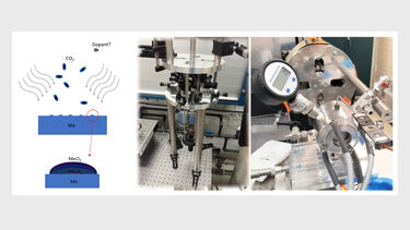
The approach at Tampere uses pattern metal films in an environment containing super-critical CO2 (>100 Bar) in order to achieve controllable localised oxidation of the metal in the regions patented by the laser interference.
This is an entirely new approach and many parameters and variables need to be explored.
Areas that need to be explored include
- the laser pulse length
- number of pulses
- laser wavelength
- CO2 pressure
The laser interference in this case is formed using a diffractive optical element which produces a square array. The angle of incidence is around six degrees.
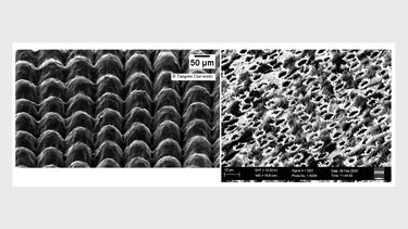
Initial studies have focused on titanium (left) and zinc (right) surfaces using four beam interference at 1064nm. It shows a good patterning capability.
The MBE approach at the University of Sheffield seeks to use in-situ laser interference to direct the growth of semiconductor structures, including quantum dots and nanowires.
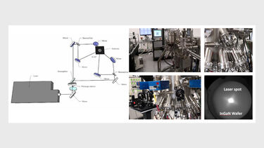
It uses a free space four beam interference set up, connected to an MBE reactor. The four beams come together on the heated substrate at 58 degrees to produce a square pattern.
We visualise the UV laser spots using a InGaN wafer, which helps us with the alignment.
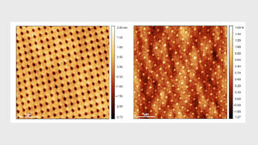
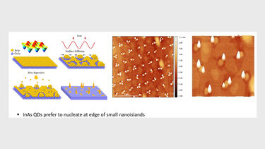
One of the most significant findings we have observed is the ability to induce both holes and islands sometimes even on the same GaAs wafer, with the same laser exposure, but at different regions of the wafer.
We believe the effect is as a consequence of different laser fluence. Islands are generated by diffusion towards the cool regions of the pattern (interference minima) and the holes are at interference maxima due to diffusion from region of high local heat.
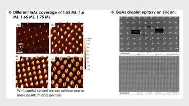
When we attempt to grow InAs quantum dots on this patterned surface, we are able to nucleate these at the edges of the nanoislands.
We have proposed a mechanism to explain this. Due to migration of indium under the influence of the thermal pattern, the indium moves towards the island where it reaches a step edge. The step edge is a preferential site for nucleation.
We have subsequently been able to demonstrate excellent control over site occupancy. We have extended this work to include patterned droplet nucleation on Silicon substrates.
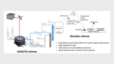
Work at CIET has focussed on the development of a new technique we call Laser Enhanced Aerosol Assisted Chemical Vapor Deposition (LEAACVD). This uses an interference laser pattern to enhance CVD growth.
Since this approach is very new, it has required much experimentation with the laser conditions, but is now showing good results.
The approach uses a small reaction vessel to which laser light is applied to the substrate (typically a metal film or silicon substrate) via a large glass window.
The approach uses a DOE to achieve the interference pattern. The reactant gas is passed through an atomiser and fed into the reaction vessel. This is where its reaction rate at the substrate is controlled by the laser pattern induced temperature gradient.
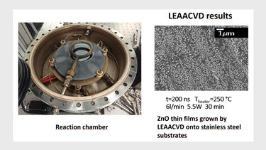
The figure shows the reaction vessel after growth and the results of ZnO growth. This is laser assisted, but without the interference.

