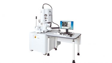
Scanning Electron Microscopy
JEOL JSM 7900F
Unique flexible platform that combines the ultimate in high resolution imaging with unparalleled nano scale microanalysis. This tool excels in lightning fast data acquisition through simple and semi-automated operation.
USES/APPLICATIONS
Applications include imaging and analysis of metals, magnetic materials, semiconductors, ceramics, medical devices, and biological specimens.
DETAILED DESCRIPTION
The JSM-700F is equipped with a large specimen chamber that accommodates a wide variety of detectors simultaneously, including:
- Secondary and back scattered electron imaging detectors,
- EDS for chemical analysis [Oxford Instruments Aztec Xmax-170],
- EBSD for orientation mapping [Oxford Instruments Aztec HKL Advanced Symmetry System],
- Transmission Bright-field,
- Dark field STEM capabilities.
The un-lens Schottky field emission gun (FEG) provides improved brightness, smaller probe sizes with increased probe current for improved analytical performance.
The Super Hybrid lens enables observation of specimens at ultra-high spatial resolution including magnetic and insulating materials.
The new Gentle Beam Super High mode (GBSH) enables a bias voltage of up to 5 kV to be applied to the specimen stage, which decreases charging on nonconductive specimens; improves spot size at low kV; enhances surface tomography; and further enables high-resolution imaging at extremely low voltages.
DETAILED SPECIFICATIONS
- Resolution: 7Å @ 1 kV, 6Å @15 kV, 6 Å in STEM
- Analytical resolution sub 30 nm scale
- Probe current > 500nA
- High sensitivity BE detector providing exceptional performance at low accelerating voltages
- Ultralow kV in-lens detectors
- GBSH-S (GENTLEBEAMTM Super High mode) enabling high resolution imaging at extremely low accelerating voltages (down to 10V)
- In-lens Schottky Plus field emission electron gun and low aberration condenser lens provide high levels of brightness
- Super Hybrid Lens (SHL), a combination of electrostatic and electromagnetic lenses, to support ultra high resolution imaging and analysis of various samples ranging from magnetic materials to insulators
- Ample prove current is available at low accelerating voltage, supporting various applications from high resolution imaging to high speed elemental mapping
- A new sample exchange system is designed to change samples in a safe, speedy, seamless manner through simple operations
- Oxford Instruments Aztec Live Energy Advanced Xmax170 X-Ray EDS System
- Oxford Instruments Aztec HKL Advanced Symmetry EBSD System
LOCATION
Sorby Centre for Electron Microscopy, The University of Sheffield North Campus, Kroto Research Institute, Broad Lane, Sheffield, S3 7HQ
ENQUIRE HERE: royce@sheffield.ac.uk

